Solar Panels As Doped Ga Doped

Pdf Lifetime Instabilities In Gallium Doped Monocrystalline Perc Silicon Solar Cells

Gallium Doped Monocrystalline Silicon Best Solution For Letid And Lid In Perc Cells Pv Tech
Gallium Doped Monocrystalline Silicon Fully Solves The Problem Of A Perc Module S Lid Pvtime

Ja Solar To Combat Cell Lid Issues With Ga Doped P Type Crystalline Silicon Wafers Pv Tech

Negligible Hysteresis Planar Perovskite Solar Cells Using Ga Doped Sno2 Nanocrystal As Electron Transport Layers Sciencedirect

Combinatorial Sputtering Of Ga Doped Zn Mg O For Contact Applications In Solar Cells Sciencedirect

Shin etsu chemical holds a number of patents on doping ga in silicon crystals and using the ga doped p type crystalline silicon wafers for making solar cells.
Solar panels as doped ga doped.

Ga Doped Zno As An Electron Transport Layer For Pffbt4t 2od Pc70bm Organic Solar Cells Sciencedirect

Ge Doped Cu2znsns4 An Investigation On Absorber Recrystallization And Opto Electronic Properties Of Solar Cell Sciencedirect

A Ga Doped Sno 2 Mesoporous Contact For Uv Stable Highly Efficient Perovskite Solar Cells Journal Of Materials Chemistry A Rsc Publishing Doi 10 1039 C7ta07663k

General Rules Of The Sub Band Gaps In Group Iv Si Ge And Sn Doped I Iii Vi2 Type Chalcopyrite Compounds For Intermediate Band Solar Cell A First Principles Study Sciencedirect

Diffusion Induced Doping Effects Of Ga In Zno Ga Zno And Azo Ga Azo Multilayer Thin Films Sciencedirect

Longi Goes In For Patent Agreement On Gallium Doped Tech Taiyangnews

Surface Engineering Of Zno Electron Transporting Layer Via Al Doping For High Efficiency Planar Perovskite Solar Cells Sciencedirect

Adsorption Of Sugars On Al And Ga Doped Boron Nitride Surfaces A Computational Study Sciencedirect

Ja Solar To Offer Customers High Quality Solar Modules With Mono Perc Mbb Cells Adopting Ga Doped Silicon Wafers Solarpv Expert

Influence Of Ga Dopant On Photoelectrochemical Characteristic Of Ga Doped Zno Thin Films Deposited By Sol Gel Spin Coating Technique Huang 2017 Surface And Interface Analysis Wiley Online Library

Structural Morphological Optical And Electrical Properties Of Ga Doped Zno Transparent Conducting Thin Films Sciencedirect

Fabrication Of P Type Conductivity In Sno2 Thin Films Through Ga Doping Sciencedirect
Https Iopscience Iop Org Article 10 1088 1361 6528 Ab1739 Pdf

Review On Alkali Element Doping In Cu In Ga Se2 Thin Films And Solar Cells Sciencedirect

Ga Doped Izo Films Obtained By Magnetron Sputtering As Transparent Conductors For Visible And Solar Applications Sciencedirect

Ga Doped Zno Nanorod Scaffold For High Performance Hole Transport Layer Free Self Powered Ch3nh3pbi3 Perovskite Photodetectors Sciencedirect
Https Research Aalto Fi Files 11258867 1 S2 0 S1876610216305008 Main Pdf

Low Temperature Grown Zno Ga Films With Predominant C Axis Orientation In Wurtzite Structure Demonstrating High Conductance Transmittance And Photol Rsc Advances Rsc Publishing Doi 10 1039 C5ra22288e

Abrupt Conversion Of The Conductivity And Band Gap In The Sputter Grown Ga Doped Zno Films By A Change In Growth Ambient Effects Of Oxygen Partial Pressure Sciencedirect
Structural Optical And Electrical Evolution Of Al And Ga Co Doped Zno Sio 2 Glass Thin Film Role Of Laser Power Density Rsc Advances Rsc Publishing Doi 10 1039 C7ra04963c

First Principles Study Of Structural Stability Electronic And Optical Properties Of Ga Doped Mapbi3 Sciencedirect

Effective Lifetimes Of Minority Carriers In Time Resolved Photocurrent And Photoluminescence Of A Doped Semiconductor Modelling Of A Gainp Solar Cell Sciencedirect

Thin Film Gaas Solar Cell Lumerical Support

The Complexity Of Lid Letid And Hid Pv Tech

Growth Of Ga Doped Zno Films By Thermal Oxidation With Gallium And Their Optical Properties Aip Advances Vol 7 No 5

Exceeding 20 Efficiency With In Situ Group V Doping In Polycrystalline Cdte Solar Cells Request Pdf

Role Of Dopant Ga In Tuning The Band Gap Of Rutile Tio2 From First Principles Sciencedirect
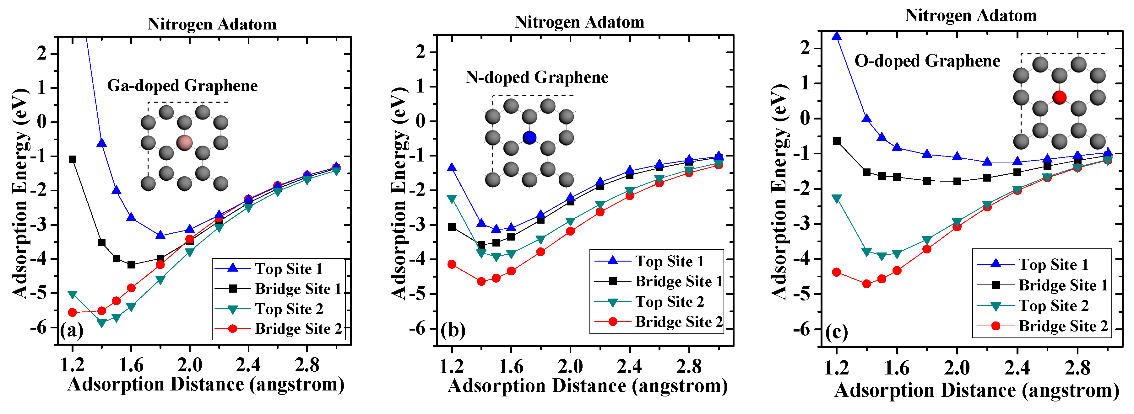
Crystals Free Full Text Strain Effects In Gallium Nitride Adsorption On Defective And Doped Graphene First Principles Calculations Html
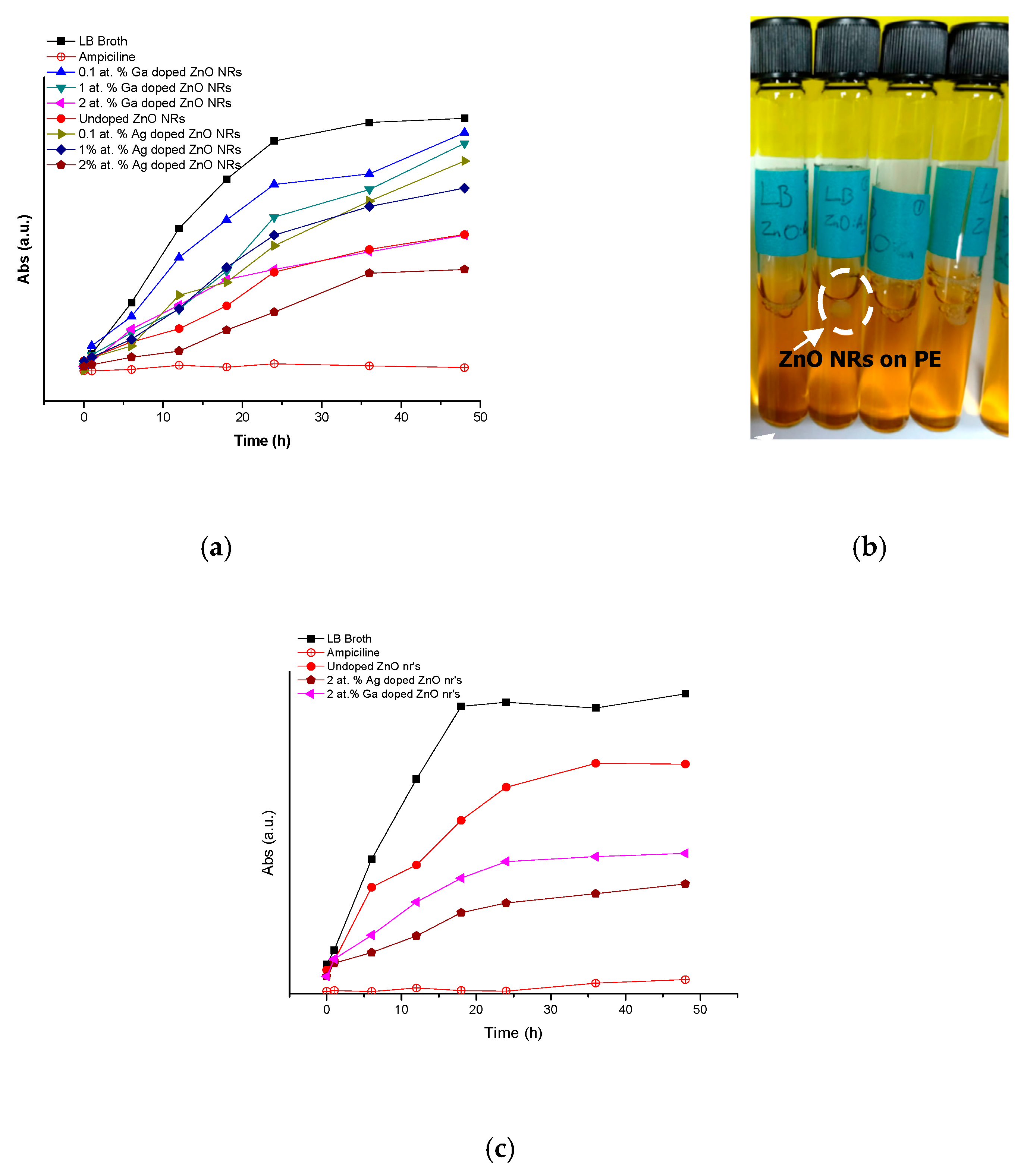
Catalysts Free Full Text Photocatalytic And Antimicrobial Properties Of Ga Doped And Ag Doped Zno Nanorods For Water Treatment Html

Excitonic Emission In Heavily Ga Doped Zinc Oxide Films Grown On Gan Sciencedirect
Https Www Sciencedirect Com Science Article Pii S1876610217339292 Pdf Md5 45cfe2af4c92063921df8a73de378399 Pid 1 S2 0 S1876610217339292 Main Pdf

Xps And Uv Vis Studies Of Ga Doped Zinc Oxide Nanoparticles Synthesized By Gelatin Based Sol Gel Approach Sciencedirect
Conducting Al And Ga Doped Zinc Oxides Rapid Optimisation And Scale Up Journal Of Materials Chemistry A Rsc Publishing Doi 10 1039 C6ta03364d

Pdf Self Compensation In Semiconductors The Zn Vacancy In Ga Doped Zno

United States

Al Doped Zno Thin Films Grown Onto Ito Substrates As Photoanode In Dye Sensitized Solar Cell Sciencedirect
Http Pubs Acs Org Doi Pdfplus 10 1021 Acsami 7b03262

Pulsed Laser Deposition Of Ga Doped Zno Films Influence Of Deposition Temperature And Laser Pulse Frequency On Structural Optical And Electrical Properties Sciencedirect

Electronic And Surface Properties Of Ga Doped In2o3 Ceramics Sciencedirect
Doped Layer An Overview Sciencedirect Topics

Metal Organic Framework Doped Spiro Ometad With Increased Conductivity For Improving Perovskite Solar Cell Performance Sciencedirect

Large Enhancement Of X Ray Excited Luminescence In Ga Doped Zno Nanorod Arrays By Hydrogen Annealing Sciencedirect
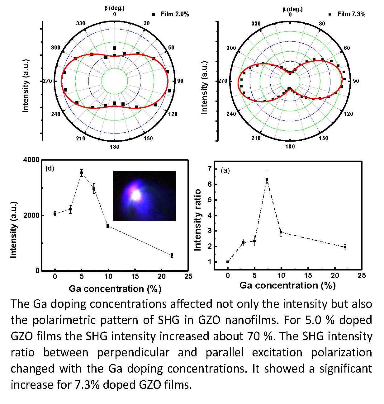
Nanomaterials Free Full Text Influences Of Ga Doping On Crystal Structure And Polarimetric Pattern Of Shg In Zno Nanofilms Html

A Downshifting Eu3 Doped Glass Embedded With Concave Pyramid Microstructure To Improve The Efficiency Of Silicon Solar Cell Sciencedirect
Source : pinterest.com
